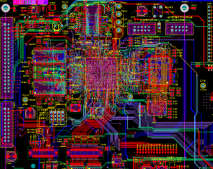
PCB layout is provided with experience in high density multi layer (up to 12 layers) designs optimised for performance, reliability and manufacturing cost. Altium Designer provides is an excellent tool providing many advanced layout tools that save layout time.
We have extensive experience with many high density complex PCB designs. Many of our designs have utilised the following technologies :
- Mutli layer up to 12 layers
- Fine pitch BGA devices
- Controlled impedance routing
- Matched length tracks
- Micro strip lines
- data speeds up to 3 GHz
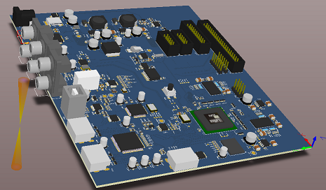

We inspect internal layers and component clearance in 3D. Altium also integrates well with Mechanical tools such as SolidWorks allowing 3D Model exchange to ensure electronics and mechanical parts are precisely integrated.
This allows us to fully investigate your full product before anything is manufactured. The result is your product is manufactured right first time with no surprises !
